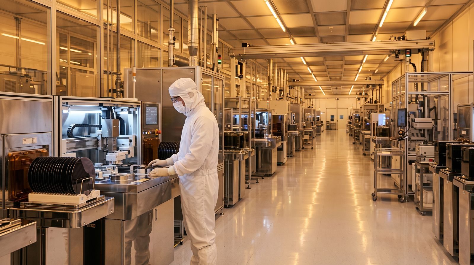
Sony Semiconductor Solutions and TSMC have signed a binding definitive agreement to build a next-generation image sensor plant in Japan, converting a May memorandum of understanding into a joint venture with a combined investment of roughly ¥1 trillion — about $6.4 billion.
The venture is called Advanced Vision Semiconductor Manufacturing Corporation. It will sit in Koshi City, Kumamoto Prefecture, inside Sony’s existing image sensor campus. Sony’s chip unit takes a controlling stake of roughly 60%; TSMC holds the remaining 40%. Sony is contributing approximately ¥465 billion through a mix of cash and transferred assets; TSMC is contributing approximately ¥282 billion in cash.
Production is targeted for 2029.
The unusual part is the 40%
TSMC does not normally take minority equity in someone else’s fab. Its entire model is to own the capacity, run it at scale, and rent it to everyone — that neutrality is the moat. Taking 40% of a plant that a single customer controls is a departure, and it means the demand signal here was strong enough to justify bending the model.
Sony’s side is easier to read. It is the dominant supplier of image sensors, its Kumamoto campus is already the centre of gravity for that business, and the capital required for the next process generation has outrun what one company comfortably funds alone. Splitting the bill with the foundry that would otherwise be a supplier converts a cost line into a shared one.
Our take: This is a bet on cameras that are not for people. Both companies point at automotive and robotics as the demand source — sensors that feed machine perception, not photographs. That market is real but unsized, and 2029 first production means the two of them are committing capital roughly three years ahead of knowing whether the volumes show up. Sony can carry that risk on its existing sensor franchise. TSMC’s 40% is the more interesting signal, because it is the party with the best view of everyone else’s order book.
Why 2029 matters
Three years is a long lead time in a market where the customers — autonomous driving programmes and humanoid robotics firms — keep resetting their own timelines. The plant either arrives into a supply shortage or into a segment that has slipped again.
What makes the timing less reckless than it looks is the location. Kumamoto is already Japan’s semiconductor cluster, with TSMC operations and a supplier base built out over the last several years. Adding a fab to an existing campus with existing utilities, existing staff pipelines and an existing customer relationship is a materially cheaper bet than a greenfield site — which is roughly the argument every fab operator is making about co-location right now.
What to watch
- The funding gap. The disclosed contributions total about ¥747 billion against a roughly ¥1 trillion programme. How the balance is financed — debt, later tranches, or Japanese government support — is not yet spelled out.
- Whether TSMC repeats the structure. If minority stakes in customer-controlled fabs become a pattern rather than an exception, the foundry model is changing.
- Automotive design wins between now and 2029. Sensors get specified years before volume. The order book, not the groundbreaking, tells you whether this plant is full.
Two companies just committed roughly $6.4 billion to a product category whose biggest customers do not exist at scale yet. That is either early or it is the whole point.