SEMICON Taiwan opened its International Semiconductor Week forums in Taipei on Monday, drawing more than 100,000 semiconductor professionals from 65 countries. The framing the organisers chose for the week is the interesting part: system architecture, not individual chip performance, is now the bottleneck in AI.
The specific claim underneath that is harder than it sounds. In today’s large AI systems, moving data between components can consume more energy than the computation the data was moved for. Not a rounding error against compute — more than it.
The arithmetic behind the problem is unforgiving. An AI cluster has to shift data between thousands of GPUs, switches and memory systems at rates exceeding 100 terabits per second per node. Copper cannot keep doing that. Electrical signalling over copper needs equalisation and retiming circuits whose power draw scales with the data rate, and signal integrity degrades with distance. Push the rate up and you pay twice, in watts and in reach.
The fix is optical, and it moves into the package
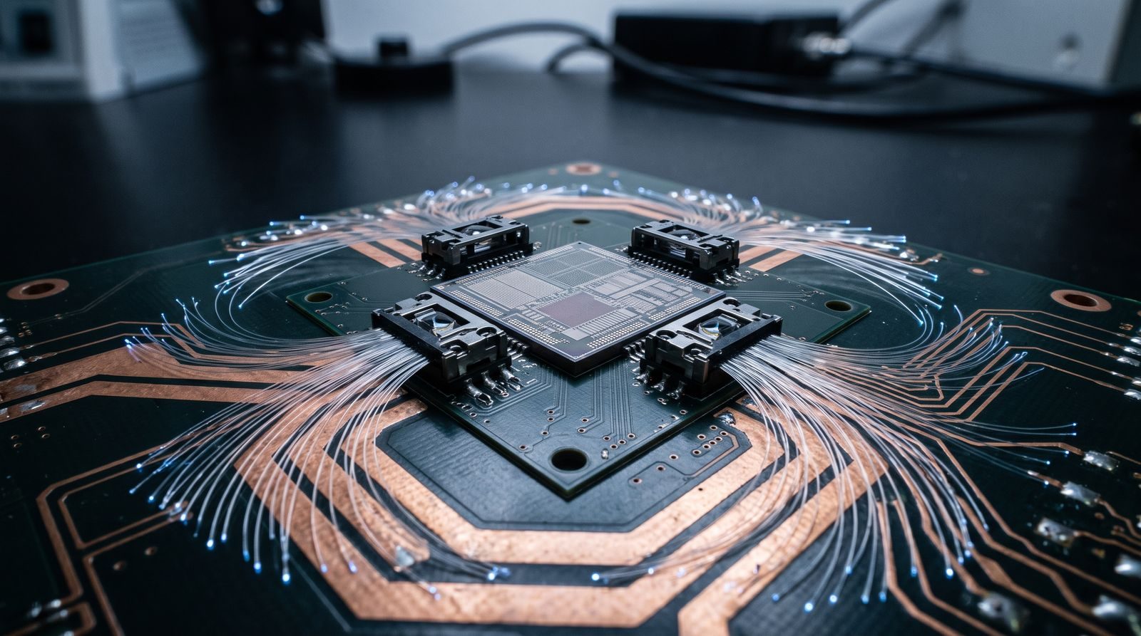
The leading engineering response is co-packaged optics: stop running electrical signals out to a pluggable transceiver at the faceplate and instead integrate the optical engines directly inside the switch ASIC package, next to the die. Shorter electrical path, more bandwidth, less power. SEMICON Taiwan gave silicon photonics its own pavilion this year, alongside an AI Technology Zone for ASIC and chip design and a Memory Executive Summit for high-bandwidth memory.
The commercial signal is that this is leaving the research track. AUO Group’s Daxin Materials subsidiary used the show to demonstrate a system-level Micro LED co-packaged optics module aimed at short-reach AI data centre interconnects of up to 10 metres — rack-scale and row-scale distances, not long haul. That is exactly the segment where copper is failing first and where the volume is.
Our take: Almost every AI capex forecast in circulation is built on a count of accelerators. If the binding constraint is data movement and the power it costs, those forecasts are measuring the wrong thing, and the value migrates down the stack — to advanced packaging, optical engines, photonics materials and the handful of firms that can manufacture them at yield. It also reframes the power story. We have been writing about data centres outrunning the grid as a siting problem. Some meaningful share of that demand is not compute at all. It is the tax on shuttling bits between chips that are sitting inches apart.
There is a second-order point for anyone reading the AI infrastructure trade. A bottleneck that sits in packaging rather than lithography has a different competitive shape. Fewer of the advantages that accrue to a leading-edge foundry apply, and more of them accrue to whoever can integrate optics, substrate and thermal design into one part that works reliably in a rack for five years. That is a materials and manufacturing problem, and it is a slower one to solve than a die shrink.
What to watch
- CPO commercialisation dates from the switch vendors. Demonstrations at a trade show and volume parts with a yield number are very different things.
- Which ceiling binds first. HBM supply and optical packaging capacity are both constrained. The one that runs out first sets the real pace of cluster buildouts.
- The 10-metre band. If short-reach optics is where copper breaks, rack-scale interconnect becomes a distinct product category with its own suppliers and its own margins.
- Energy accounting. If data movement really is the larger share, expect the disclosed power-usage figures for AI facilities to start being broken out differently.